
Gizmo_Duck
blathering blatherskite!

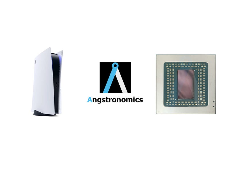
With an exclusive side-by-side comparison showing 6nm Oberon Plus next to 7nm Oberon, we can see what has physically changed in the 2 years between them. Die size has gone from ~300 mm² to below 260 mm², a shrink of close to 15%. What this means in the end is that each wafer processed can produce near 20% more chips for a similar cost.
more at the link:For this example, TSMC ensures that their 6nm EUV process is Design Rule Compatible with their N7 DUV process, meaning that customers can reuse existing designs made for N7 to use on N6, with a simple conversion process that does not alter the underlying high-level synthesis.

This pretty much means that everyone that wants a PS5 will be able to get one pretty soon. As of early next year (after the holidays) they should be regularly seen on shelves. This has already gone into effect and its been shipped in certain territories already. It should start to roll out in the the west in October.
Not only will it produce a lot more PS5’s but it will have a sign finally less power draw. Its most likely why there are making a redesign in 2024. This is also the reason Sony forecasted they’d be able to ship 18.7m consoles this fiscal year. Seems like production is ready to take off.


